Modern electronics have come to rely heavily on printed circuit boards. A typical computer may have several PCBs including one complex board called the "motherboard." Individual components can be attached to this board and connected together with a pattern of copper lines covering the board which create pathways for the electricity to travel between components.
Electrical Pathways
Video of the Day
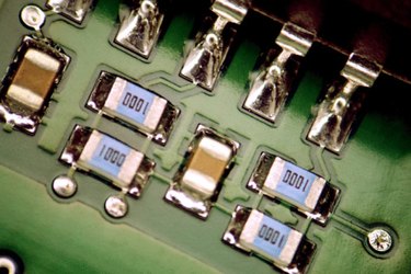
The electrical pathways or conductors are made up of two different parts. The first part is the lines themselves and they are called "traces." The second part is called a "land" or "pad." A land is a conductive surface providing a place on which to attach various components, make a connection or provide a test site.
Video of the Day
Single-Layer Printed Circuit Boards
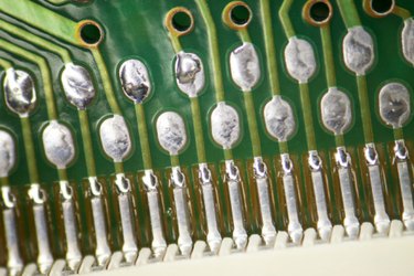
Original circuit boards were simply a single-sided circuit board. The board itself is non-conductive but the traces started out as a solid layer of copper and then the spaces in-between were etched away with a chemical bath. Component leads were inserted through holes, soldered from the back and clipped off short.
Double-Sided Laminate
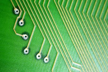
In an effort to conserve space the double-sided board was invented. By mounting components to the surface of the board rather than using holes, both sides of the circuit board could be used. Holes plated through the board, called a "via," conduct electricity from one side of the board to the other.
Multi-Layer
Further advances came as PCB manufacturers were able to create internal layers that would also conduct electricity allowing even more complex circuit design. This is achieved through a sandwich type of construction. Vias can be designed to only go part way through the board to carry electricity to the internal layers.